Slide 1

-Passive and active photonic components
- Full PIC design, layout, validation and tapeout
- Photonic PDK development

- Passive and active photonic components
- Full PIC design, layout, validation and tapeout
- Photonic PDK development

- Passive and active photonic components
- Full PIC design, layout, validation and tapeout
- Photonic PDK development

Custom Photonic PIC Design
previous arrowprevious arrow
next arrownext arrow
    Rymoslite specializes in custom PIC chip development, offering expertise in passive and active photonic component design, full PIC design and tape-out, PDK development and multi-product wafer (MPW) submission to photonic foundries.
    Our services also include photonic package development, including RF substrate or interposer design and fiber-to-chip coupling. We can do feasibility studies for your photonic project starting from concept development to prototyping by identifying photonic foundry and packaging partners. Below are our key expertise.
    • Custom Integrated Photonic Chip (PIC) Development
    • Photonic Package Design: Optical and RF design
    • Photonic Consulting

Photonic integrated circuit design, simulation and analysis

Co-package optics: Shows one edge of electronic ASIC interfacing with 4-photonic modules.

Let's talk about your PIC project

Drop us a line below or email at info@rymoslite.com
My Website - Photonic Chip Visualization
>

Photonic System Design Meets AI
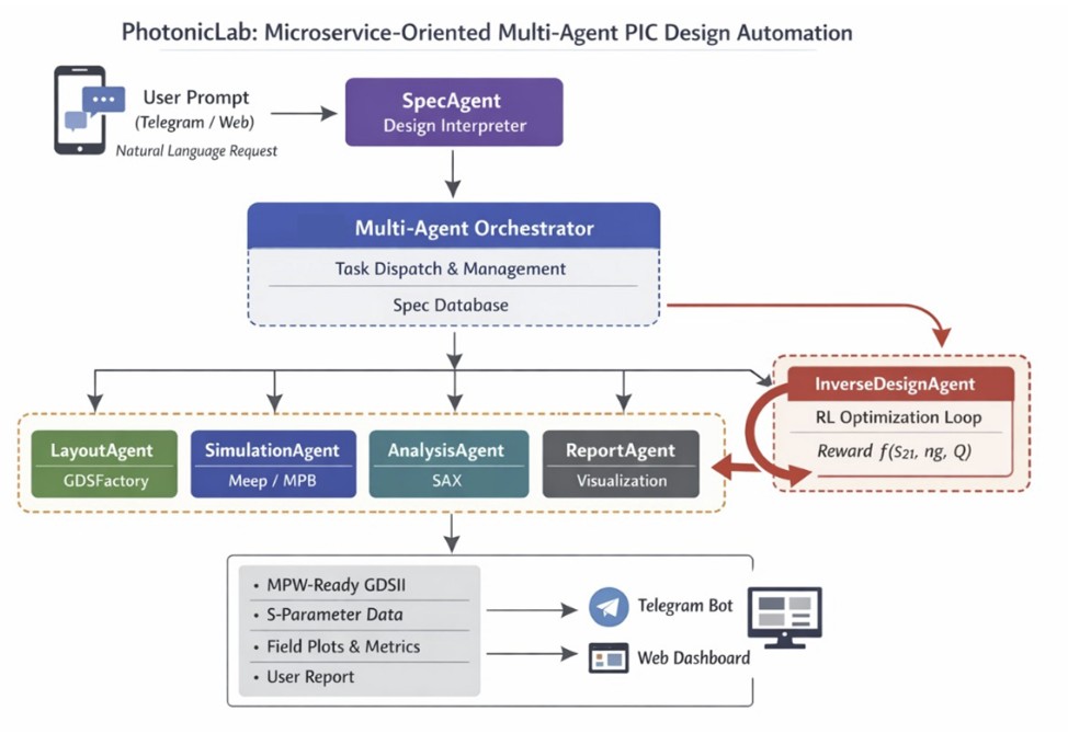
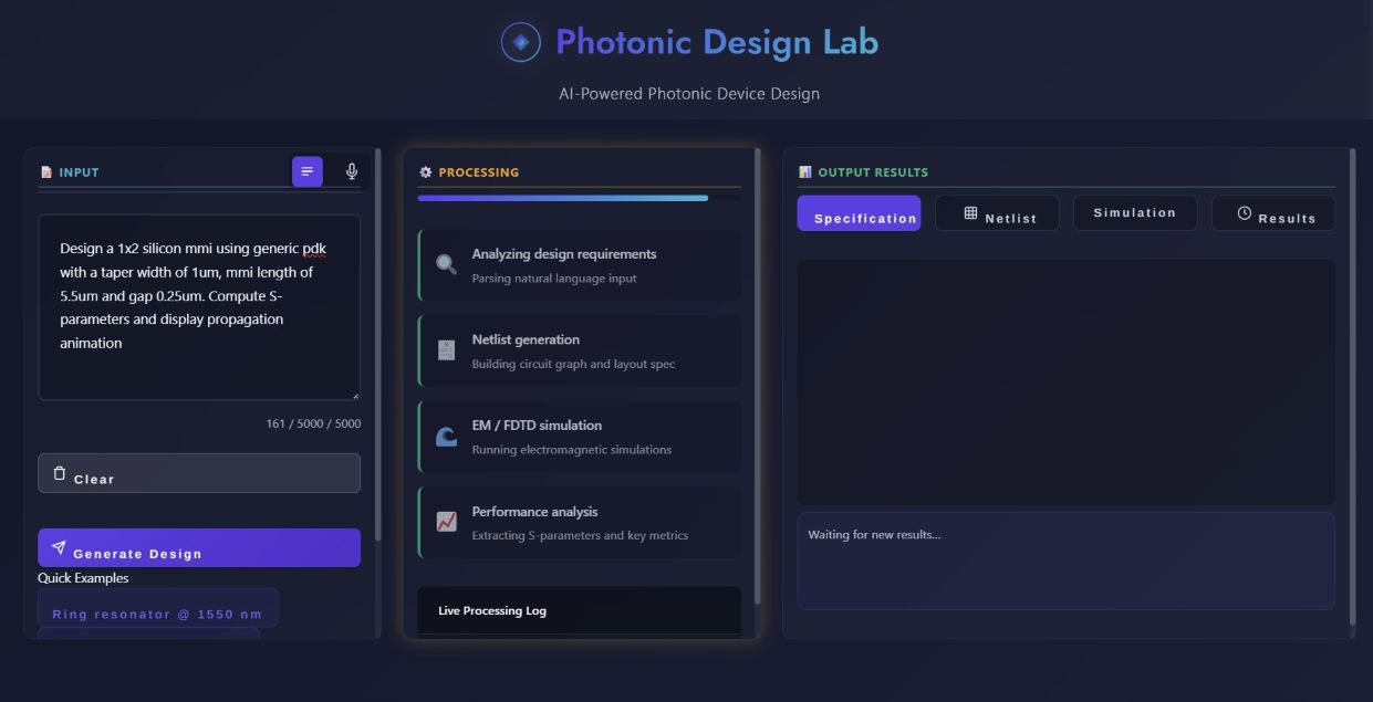
Custom PIC development from concept to tape-out. We transform optical innovation into manufacturable photonic integrated circuits with unmatched precision and expertise.

Our Services

End-to-end photonic solutions tailored to your specifications

Custom PIC Development

Complete photonic integrated circuit design from initial concept through final fabrication. We handle every stage of the development process with precision
🔬

Component Design

Expert design of passive and active photonic components including waveguides, modulators, detectors, and coupling structures optimized for your application.
🎯

Full Design & Tape-Out

Comprehensive PIC layout, verification, and tape-out services ensuring your design meets foundry specifications and manufacturing requirements
📐

PDK Development

Custom Process Design Kit creation and optimization, enabling efficient design workflows and ensuring compatibility with target fabrication processes.
🏭

MPW Coordination

Multi-project wafer submission management to leading photonic foundries, reducing costs while maintaining quality and timeline commitments.
🔧

Technical Consulting

Strategic guidance on photonic integration challenges, technology selection, and design optimization for commercial and research applications.

AI Assisted Photonic Circuit Design

Watch how we bring your photonic designs to life

Passive design of photonic integrated circuit building blocks

Waveguide, MMI, ring

Thin Film Lithium Niobate with Capacitive-Loaded Traveling Wave Electrodes (CLTWEs)

Custom Photonic Chp Development and Optical Interconnect Prototyping

Photonic Design Tools Expertise

Deep knowledge across the photonic integration stack

  • Photonic

    -Ansys Lumerical, Tidy3d, Comsol, etc.

    - Python based open-source Tools: GDSFactory, SAX, Meep/MPB, etc.

  • RF Design

    - Ansys HFSS, Circuit, COMSOL multi-physics,etc.

    - open source and custom developed tools.

  • Design Automation

    - Custom scripting and automated design flows to accelerate development cycles and ensure design consistency.

  • 3D Cad Tools

    Mechanical, Opto-mechanical: Solidworks, Zemax Optical Stud.

Ready to Build Your Photonic Solution?

Let's discuss how we can bring your photonic integrated circuit from concept to reality. Our team is ready to tackle your most complex design challenges.

Get in Touch